Hi Friends! Here, we will explain about SRAM circuit design and operation | SRAM working architecture; as well as SRAM read and write operation with circuit diagram in detail. This is unique post over the internet. So we make ensure that at the end of this article; you will definitely fully aware about SRAM Circuit Design and Operation without getting any hassle.
Definition: Full form of SRAM is “Static Random Access Memory” in Computer industry. SRAM is also simple types of RAM (Random Access Memory) that helps to store all data with using of static technique. Static RAM is able to retain all information into static form until power supply is turn off, so due to this nature this memory is known as volatile memory.
SRAM is totally different to DRAM because DRAM requires regularly refreshing data that is store in the memory. So, SRAM’s speed is fastest to DRAM as well as it consume less power to DRAM.
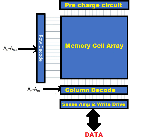
SRAM Block Diagram
In SRAM, All data has been stored in flip-flop. Flip-flop contains the every bit of this Ram. Flip-flop uses 4-6 transistors for making a memory cell and its circuit do not need to refreshment continuously. SRAM helps to store every bit with using of bistable latching circuitry, and typically it used six MOSFET to store every memory bit but extra transistor become at smaller nodes.
SRAM holds a bit of data on 4 transistors with using of 2 cross coupled inverters, and it has two stable states like as 0 and 1. Due to read and write operations, other two access transistors are used to handle the availability for memory cell. It needs 6 MOFSET (metal-oxide-semiconductor field-effect transistor) to hold per memory bit. MOFSET is also one type of SRAM chip, and other is bipolar junction transistor. Bipolar junction transistor’s speed is fastest but it uses much power.
Examples – Unsaved PPT file in PowerPoint and other any unsaved data in the software
SRAM Circuit Design and Operation
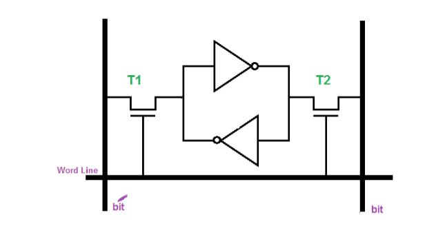
Static Random Access Memory cell is designed with two inverters, which are cross-linked like as latch form. This latch is made connection to two bit line along with two transistors T1 and T2. Now both transistors are capable to alter their modes (open or close) under control of word line, and this entire process is controlled by address decoder. When word line goes to ground level then both transistors get turned off, and latch starts to retain own state.
SRAM Circuit Diagram
How Does Work Static RAM?
In this section, we will cover about complete working structure of SRAM in detail, as follow them:
SRAM Read and Write Operation
Static RAM working is divided into three operations like as Read, Write and Hold.
SRAM Read Operation:
Both switches T1 and T2 are closed while activating the word line. When, cell comes to state 1 then signal flows in high amount on b line and other side signal flows in low amount on b’ line. Opposite is true when cell goes to state 0. Finally both b and b’ get complement of each other’s.
Sense/write, which are connected in the rear side of two bit line, they monitor their states and finally convert into output respectively.
SRAM Write Operation:
In the write operation, Sense/Write circuit allows to drive bit lines b and it complement b’, and then it provides accurate values on bit line b and b’ as well as go to activate word line.
SRAM Hold Operation:
For Hold Operation both access transistors must be turn OFF (T1 and T2). Due to presence of latching element SRAM hold its state.
FAQs (Frequently Asked Questions)
What is the primary function of SRAM in electronic circuits?
The primary function of SRAM is to provide fast and temporary data storage in electronic circuits. It is often used as cache memory in processors to store frequently accessed data.
How is SRAM different from DRAM in terms of circuit design?
SRAM and DRAM differ in their basic cell structure. SRAM cells use flip-flops, typically composed of multiple transistors, while DRAM cells use capacitors and require refreshing circuits.
What is the significance of the wordline and bitline in SRAM operation?
The wordline is responsible for selecting a row of SRAM cells, and the bitline is used for reading from and writing to individual cells within the selected row.
How is data read from an SRAM cell, and what role do sense amplifiers play?
Data is read from an SRAM cell by activating the wordline and bitlines. Sense amplifiers detect and amplify the small voltage differences on the bitlines, determining the state of the memory cell.
What challenges are associated with reducing the size of SRAM cells in the design process?
Shrinking the size of SRAM cells poses challenges such as increased leakage currents, reduced stability, and potential interference between neighboring cells.
Final Words
Through this article, you have been fully educated about SRAM circuit design and operation | SRAM working architecture; as well as SRAM read and write operation with circuit diagram in detail. If this article is helpful for you, then please share it along with your friends, family members or relatives over social media platforms like as Facebook, Instagram, Linked In, Twitter, and more.
If you have any experience, tips, tricks, or query regarding this issue? You can drop a comment!
 with Block Diagram")
? Types and Examples of ROM!")
 with Block Diagram")

? Types and Examples of ROM!")


? Examples & Types of SRAM")


