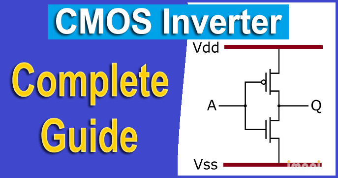
Hi Learners! From this article, we will explain all important things about what is CMOS inverter with its circuit diagram; involving with their working operations and applications of CMOS inverter with ease. This is unique article over the Internet. So, at the end of this post, you will definitely educate about CMOS Inverter without any hassle.
What is CMOS Inverter?
CMOS inverter (complementary metal-oxide-semiconductor inverter) is a fundamental building block of digital integrated circuits. This kind of field-effect transistor (FET) is using in both p-type and n-type metal–oxide–semiconductor field-effect transistors (MOSFETs). It grabs very low power consumption, higher noise immunity, and high integration density.
The inverter composes of the metal gate that lies at the top of an insulating layer of oxygen on top of a semiconductor. CMOS technology is widely going to use for constructing integrated circuit (IC) chips. This includes microprocessors, microcontrollers, memory chips, and other digital logic circuits.
CMOS Inverter Tutorial Headlines:
In this section, we will show you all headlines about this entire article. You can check them as your choice; below shown all:
What is CMOS Inverter?
CMOS Inverter Working with Operations
Applications of CMOS Inverter
CMOS Inverter Characteristics
Advantages of CMOS Inverter
Disadvantages of CMOS Inverter
FAQs (Frequently Asked Questions)
What is the threshold voltage in CMOS inverters?
What is role of the pull-up and pull-down networks in CMOS inverter?
Can CMOS inverter drive capacitive loads?
What is the significance of the switching threshold in CMOS inverters?
Are there variations of CMOS inverters?
Let’s Get Started!!
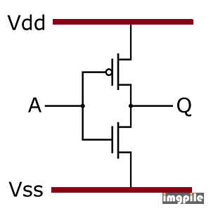
How Does CMOS Inverter Work?
The working principle of the CMOS inverter involves the operation of two complementary metal-oxide-semiconductor (CMOS) transistors: one PMOS (p-type metal-oxide-semiconductor) transistor and one NMOS (n-type metal-oxide-semiconductor) transistor. These transistors make connection in series, creating a basic inverter circuit.
Explanation About CMOS Inverter Working with Operations:
Input Signal (In)
The input signal (In) apply to both the PMOS and NMOS transistors. The input can be either a logic high (1) or a logic low (0).
PMOS Transistor Operation (P-Channel MOSFET)
When the input signal is at a logic low (0):
The PMOS transistor gets turn ON. It conducts current from the power supply voltage (Vdd) to the output (Out).
The PMOS transistor has a p-type channel and conducts when a negative voltage applied to its gate relative to its source.
The current flow pulls the output voltage (Out) to Vdd.
NMOS Transistor Operation (N-Channel MOSFET)
When the input signal is at logic high (1):
The NMOS transistor gets turn ON. It conducts current from the output (Out) to the ground (GND).
The NMOS transistor has an n-type channel and conducts when a positive voltage apply to its gate relative to its source.
The current flow pulls the output voltage (Out) to GND.
Output Voltage (Out)
The output voltage (Out) taken from the connection point of the PMOS and NMOS transistors.
The complementary actions of the PMOS and NMOS transistors result in an inverted output. When the input is low, the output is high, and vice versa.
Truth Table for CMOS Inverter Logic Gate
CMOS inverter is also known as a NOT gate; it is fundamental logic gate in digital electronics that inverts the input signal. This truth table shows that when the input is 0, the output is 1, apposite when the input is 1, the output is 0. This behaviour is getting to reflect the fundamental function of CMOS inverter that is to produce an output that is the logical negation of its input.
Input (A)
Output (B)
0
1
1
0
Applications of CMOS Inverter
The CMOS inverter finds applications in various areas due to its advantageous characteristics. Some of the key uses cases of CMOS Inverter include:
Digital Integrated Circuits: CMOS inverters are fundamental building blocks in digital integrated circuit design, including the construction of various digital logic gates such as AND, OR, and XOR gates, as well as flip-flops and microprocessors.
Memory Devices: CMOS technology is widely using in the design of computer memories, including RAM, ROM, and EEPROM. The low power dissipation and high noise immunity of CMOS inverters make them suitable for memory applications.
Microcontrollers and Microprocessors: CMOS technology, including CMOS inverters, is the dominant semiconductor technology for microprocessors, microcontroller chips, and Application-Specific Integrated Circuits (ASICs).
Low-Power Applications: Due to their low static power consumption, CMOS inverters are using in low-power applications such as portable electronic devices, battery-operated systems, and energy-efficient electronics.
Digital Signal Processing: CMOS inverters are also using in digital signal processing applications, including filters, amplifiers, and modulators.
Analog-to-Digital Converters: CMOS inverters can use in the design of analog-to-digital converters, which convert analog signals into digital signals.
Timers and Counters: CMOS inverters uses in the design of timers and counters, which are essential components in digital systems.
Clock Generators: CMOS inverters can also use in the design of clock generators, which generate clock signals for digital systems.
Data Storage and Retrieval: This inverters are applying in the design of data storage and retrieval systems, including hard drives and solid-state drives.
Wireless Communication Systems: CMOS inverters are also utilise in the design of wireless communication systems, including Bluetooth, Wi-Fi, and cellular communication systems.
CMOS Inverter Characteristics
The CMOS inverter characteristics define with its voltage transfer characteristics (VTC) that shows the relationship in between the input and output voltages. The VTC of a CMOS inverter characterized by higher noise immunity and low static power consumption. Here are some important facts about CMOS inverter characteristics:
High Noise Immunity:The CMOS inverter has a high input resistance around the threshold voltage, which makes it less susceptible to noise. This is because the input signal is applied to the gate of the transistors, which has high impedance.
Low Static Power Consumption: The CMOS inverter consumes low static power because the transistors are either fully on or fully off, depending on the input signal. Only a small amount of power is consumed when the transistors are in the saturation region, which occurs when the input is close to the threshold voltage.
Voltage Transfer Characteristics (VTC):The VTC is a plot of the output voltage versus the input voltage. The VTC has a narrow transition zone, which allows for high gain. The VTC is characterized by three regions:
Subthreshold Region: When the input is below the threshold voltage, the pMOS transistor is off, and the nMOS transistor is on. The output voltage is low.
Saturation Region: When the input is close to the threshold voltage, both the pMOS and nMOS transistors are in the saturation region. The output voltage drops drastically from Vdd.
Linear Region: When the input is above the threshold voltage, the pMOS transistor is on, and the nMOS transistor is off. The output voltage is high.
Input and Output Voltage Levels: The input and output voltage levels are typically defined as follows:
Input High (Vin = Vdd): The output is low (Vout = 0).
Input Low (Vin = 0): The output is high (Vout = Vdd).
Threshold Voltage (Vth): The threshold voltage is the voltage at which the transistor starts to conduct. For a CMOS inverter, the threshold voltage is typically Vdd/2, where Vdd is the output voltage.
Load Current: The load current is the current that flows through the output when the output is high. The load current is determined by the width and length of the transistors and the output voltage.
Power Consumption: The power consumption of a CMOS inverter is low when the transistors are in the off state. The power consumption is high when the transistors are in the saturation region, which occurs when the input is close to the threshold voltage.
Speed: The speed of a CMOS inverter is determined by the transistor sizes and the output load. The speed can be increased by using smaller transistors and lower output loads.
Logic Symbol and Truth Table: The logic symbol of a CMOS inverter is a triangle with an arrow pointing to the output. The truth table shows the input and output values for all possible input combinations.
Circuit Structure: The generalized circuit structure of a CMOS inverter consists of an nMOS transistor and a pMOS transistor connected in series. The nMOS transistor acts as a driver transistor when the input is low, and the pMOS transistor acts as a driver transistor when the input is high.
Advantages of CMOS Inverter
Here are the advantages of CMOS (Complementary Metal-Oxide-Semiconductor) inverters including:
Low Power Consumption: CMOS inverters have low static power consumption because they draw negligible current when in a stable state.
High Noise Margins: CMOS technology provides high noise margins, making the circuits robust against variations in input levels.
Wide Operating Voltage Range: CMOS inverters can operate over a wide range of supply voltages, providing flexibility in circuit design.
High Input Impedance: CMOS inverters have high input impedance, reducing the loading effect on preceding stages in a circuit.
Complementary Operation: CMOS inverters use complementary transistors (PMOS and NMOS) for switching, allowing for efficient utilization of both NMOS and PMOS transistors.
Reduced Power Dissipation during Switching: Power dissipation in CMOS circuits occurs mainly during transitions, and the symmetric pull-up and pull-down networks help minimize power consumption.
Symmetrical Rise and Fall Times: CMOS inverters typically exhibit symmetrical rise and fall times for the output signal, contributing to balanced performance.
High Integration Density: CMOS technology enables high integration density, allowing the integration of a large number of transistors on a single chip.
Ease of Fabrication: CMOS technology is well-suited for large-scale integration due to its compatibility with modern semiconductor fabrication processes.
Improved Temperature Stability: CMOS inverters tend to have good temperature stability, making them suitable for a wide range of operating conditions.
Minimal Short-Circuit Power Dissipation: The complementary nature of CMOS transistors minimizes the risk of simultaneous conduction, reducing short-circuits power dissipation.
Disadvantages of CMOS Inverter
While CMOS (Complementary Metal-Oxide-Semiconductor) inverters offer many advantages, they also have some disadvantages. Here are the essential drawbacks and limitations of CMOS Inverter, including:
Complex Fabrication Process: The fabrication process for CMOS circuits can more complex compared to some other technologies, leading to potentially higher manufacturing costs.
Limited Driving Capability: CMOS inverters may limited driving capability for heavy loads, and additional buffering may required in some cases.
Threshold Voltage Sensitivity: CMOS circuits are sensitive to threshold voltage variations, which can affect by process variations, temperature changes, and aging.
Parasitic Capacitance: Parasitic capacitance in CMOS circuits can impact performance, especially at high frequencies, leading to slower operation.
Power Consumption during Switching: While CMOS circuits have low static power consumption, they can exhibit higher power consumption during switching due to both the PMOS and NMOS transistors being momentarily conductive during transitions.
Clock Skew Issues: Clock skew, caused by manufacturing variations or environmental factors, can be a concern in high-frequency applications.
Limited Noise Immunity in Weak Pull-Up or Pull-Down: In some situations, especially when one of the pull-up or pull-down networks is weaker, noise immunity may be reduced.
Substrate Coupling Effects: Substrate coupling effects can impact the performance of CMOS circuits, particularly in mixed-signal or analog designs.
Radiation Sensitivity: CMOS circuits can be sensitive to radiation, which may be a concern in certain applications, such as aerospace or high-altitude environments.
Dynamic Power Consumption: Although CMOS circuits are power-efficient in static conditions, dynamic power consumption during transitions can be a significant factor in overall power dissipation.
FAQs (Frequently Asked Questions)
What is the threshold voltage in CMOS inverters?
The threshold voltage is the minimum input voltage required to make the transistor conduct. In CMOS inverters, the threshold voltages for the NMOS and PMOS transistors are designed to be equal, ensuring symmetrical operation.
What is the role of the pull-up and pull-down networks in a CMOS inverter?
The pull-up network consists of the PMOS transistor, and the pull-down network consists of the NMOS transistor. These networks work together with creating the inverting behaviour that making ensure the high output whenever the input is low and low output when the input is high.
Can CMOS inverter drive capacitive loads?
CMOS inverters are generally capable of driving capacitive loads, but excessive capacitance may lead to increased signal propagation delays. Buffer stages or other techniques may be employed to handle larger capacitive loads efficiently.
What is the significance of the switching threshold in CMOS inverters?
The switching threshold is the input voltage at which the output voltage transitions from high to low or vice versa. It plays the major role in determining the speed and reliability of the inverter in digital circuits.
Are there variations of CMOS inverters?
Yes! There are variations such as Schmitt trigger CMOS inverters, which have hysteresis and are useful in noise-prone environments.
Wrapping up
Now, we can hope that you have completely educated about what is CMOS inverter with its circuit diagram; involving with their working operations and applications of CMOS invertor with ease. If this post is useful for you, then please share it along with your friends, family members or relatives over social media platforms like as Facebook, Instagram, Linked In, Twitter, and more.


 with Block Diagram")

 | Working of SRAM")


